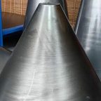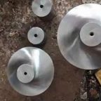
Spin forming, also known as metal spinning or spin forging, is a metalworking process that involves rotating a metal blank or tube at high speed while applying localized pressure with rollers or tools to shape it into a desired form. This technique, rooted in ancient craftsmanship, has evolved into a sophisticated manufacturing method used across industries, including aerospace, automotive, and, more recently, microelectronics. Unlike traditional forming processes like stamping or forging, spin forming is an incremental process, allowing for precise control over material deformation, reduced material waste, and the ability to work with hard-to-deform alloys. Its adaptability to produce axisymmetric components with complex geometries makes it particularly appealing for advanced applications.
Microelectronic packaging, on the other hand, is a critical discipline within electronic engineering that focuses on protecting and interconnecting integrated circuits (ICs), microelectromechanical systems (MEMS), and other nanoelectronic components. Packaging ensures electrical connectivity, thermal management, and mechanical stability while shielding delicate components from environmental stressors such as moisture, vibration, and thermal cycling. As microelectronics continue to shrink in size and increase in complexity, packaging technologies must evolve to meet demands for miniaturization, performance, and cost-effectiveness.
The intersection of spin forming and microelectronic packaging represents a novel frontier. Spin forming’s ability to produce lightweight, high-strength, and precise metallic components aligns with the need for advanced packaging solutions that support the performance and reliability of modern microelectronic devices. This article explores the principles, applications, challenges, and future prospects of spin forming technology in microelectronic packaging, providing a comprehensive analysis supported by detailed comparisons and technical insights.
Fundamentals of Spin Forming Technology
Principles of Spin Forming
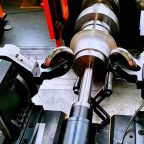
Spin forming operates on the principle of plastic deformation, where a rotating metal blank is shaped by the controlled application of force. The process typically involves a mandrel (a template that defines the final shape) and rollers that incrementally deform the material. The blank, often a flat disk or a cylindrical tube, is clamped to a rotating spindle, and rollers apply localized pressure to stretch and thin the material, causing it to flow along the mandrel’s contours.
There are two primary types of spin forming: conventional spinning and flow forming. Conventional spinning maintains the blank’s thickness while shaping it into conical, cylindrical, or hemispherical forms. Flow forming, conversely, intentionally reduces the wall thickness, enabling the production of elongated, thin-walled components with enhanced strength due to work hardening. Both techniques are relevant to microelectronic packaging, where precision and material properties are paramount.
Key Parameters in Spin Forming
The success of spin forming depends on several parameters, including:
- Rotational Speed: Determines the centrifugal forces acting on the blank and influences material flow.
- Roller Feed Rate: Controls the rate of deformation and affects surface finish and dimensional accuracy.
- Material Properties: Ductility, yield strength, and strain hardening behavior dictate formability.
- Tool Geometry: Roller shape and mandrel design influence the final component’s geometry and tolerances.
- Lubrication: Reduces friction between the roller and blank, minimizing defects like galling or cracking.
These parameters must be optimized to achieve the tight tolerances and high-quality surfaces required for microelectronic packaging components, such as heat sinks, shielding cans, or interconnect substrates.
Materials Used in Spin Forming
Spin forming is compatible with a wide range of metals and alloys, many of which are relevant to microelectronic packaging. Common materials include:
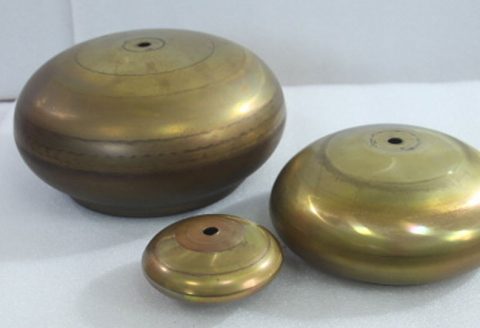
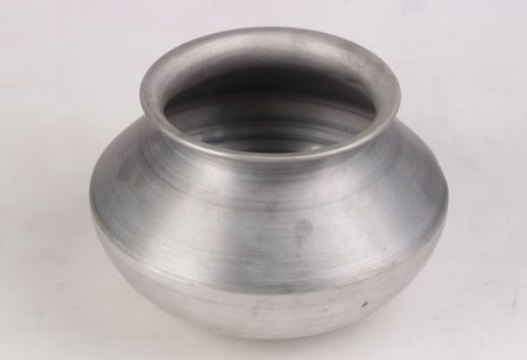
- Aluminum Alloys: Lightweight, corrosion-resistant, and thermally conductive, ideal for heat sinks and enclosures.
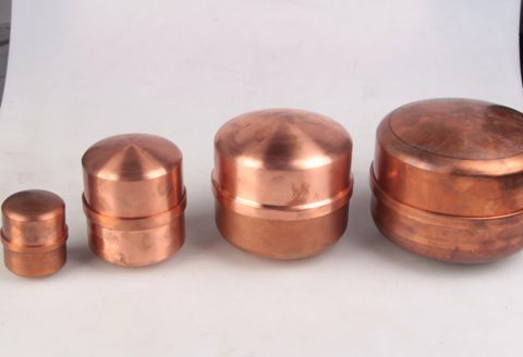
- Copper Alloys: High electrical and thermal conductivity, used for interconnects and thermal management components.
- Stainless Steel: Offers strength and corrosion resistance for robust packaging structures.
- Titanium Alloys: High strength-to-weight ratio and biocompatibility, suitable for specialized applications like bio-MEMS.
- Nickel Alloys: Excellent thermal and electrical properties, used in high-performance packaging.
The choice of material depends on the specific requirements of the microelectronic package, such as thermal conductivity, electrical performance, or mechanical durability.
Microelectronic Packaging: Requirements and Challenges
Role of Packaging in Microelectronics
Microelectronic packaging serves multiple functions, including:
- Electrical Interconnection: Providing reliable pathways for signal transmission between the IC and external systems.
- Thermal Management: Dissipating heat generated by high-performance chips to prevent overheating.
- Mechanical Protection: Shielding delicate components from physical damage and environmental stressors.
- Signal Integrity: Minimizing noise and ensuring high-speed data transmission.
- Miniaturization: Enabling compact designs to meet the demands of portable and wearable devices.
Modern packaging technologies, such as 3D integrated circuits (3D ICs), chiplet-based designs, and wafer-level packaging (WLP), push the boundaries of traditional manufacturing methods. These advancements require innovative materials and processes to achieve the necessary precision and performance.
Challenges in Advanced Packaging
The evolution of microelectronics has introduced several challenges for packaging:
- Miniaturization: As devices shrink, packaging components must maintain functionality within smaller footprints.
- Thermal Management: High-power chips generate significant heat, necessitating efficient heat dissipation.
- Material Compatibility: Packaging materials must be compatible with semiconductors and withstand thermal cycling.
- Cost-Effectiveness: Balancing performance with manufacturing costs is critical for mass production.
- Reliability: Packages must endure environmental stressors, including humidity, vibration, and temperature fluctuations.
Spin forming addresses these challenges by offering a flexible, cost-effective method to produce high-precision components with tailored material properties.
Application of Spin Forming in Microelectronic Packaging
Heat Sinks and Thermal Management Components
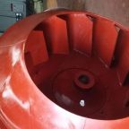
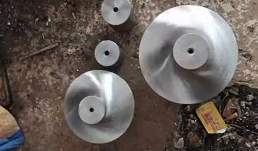
One of the most prominent applications of spin forming in microelectronic packaging is the production of heat sinks. Heat sinks are critical for dissipating heat from high-performance ICs, such as those used in data centers, 5G infrastructure, and artificial intelligence (AI) processors. Spin forming enables the creation of heat sinks with complex geometries, such as fins or radial patterns, that maximize surface area for heat dissipation.
For example, aluminum or copper heat sinks can be spun into thin-walled, lightweight structures with intricate fin designs. These components offer superior thermal conductivity and can be customized to fit specific chip layouts. The incremental nature of spin forming allows for precise control over wall thickness and surface finish, reducing thermal resistance and improving heat transfer efficiency.
Table 1: Comparison of Heat Sink Manufacturing Methods
| Method | Material | Complexity | Cost | Thermal Performance | Lead Time |
|---|---|---|---|---|---|
| Spin Forming | Al, Cu, Alloys | High | Moderate | Excellent | Short |
| Extrusion | Al, Cu | Moderate | Low | Good | Short |
| Die Casting | Al, Zn | Moderate | High | Moderate | Long |
| CNC Machining | Al, Cu, Ti | High | Very High | Excellent | Long |
Electromagnetic Shielding Cans
Electromagnetic interference (EMI) is a significant concern in microelectronics, as it can degrade signal integrity and cause device malfunctions. Spin forming is used to produce metallic shielding cans that encase sensitive components, blocking external electromagnetic fields. These cans, typically made from materials like stainless steel or nickel alloys, require precise dimensions and seamless construction to ensure effective shielding.
Spin forming’s ability to create thin-walled, seamless structures is particularly advantageous. Unlike stamped or welded cans, spun cans exhibit uniform material properties and fewer stress concentrations, enhancing durability and shielding performance. The process also allows for the integration of features like flanges or mounting tabs, simplifying assembly.
Interconnect Substrates and Lead Frames
Interconnect substrates and lead frames provide electrical connections between the IC and external circuits. Spin forming can produce cylindrical or conical substrates with integrated conductive pathways, offering an alternative to traditional flat lead frames. For instance, copper or copper alloy substrates can be spun into precise shapes with embedded conductive traces, enabling high-density interconnects for 3D ICs or chiplet designs.
The process’s flexibility allows for the creation of multi-layered structures, where different materials are spun together to combine electrical and thermal properties. This is particularly useful for advanced packaging techniques like fan-out wafer-level packaging (FOWLP), where compact, high-performance interconnects are essential.
Encapsulation Shells for Hermetic Packaging
Hermetic packaging is used in applications requiring high reliability, such as aerospace, medical devices, and military electronics. Spin forming can produce seamless metallic shells that encase ICs, protecting them from moisture, dust, and other contaminants. Materials like titanium or stainless steel are commonly used due to their corrosion resistance and mechanical strength.
Spun shells offer advantages over traditional hermetic packages, which are often assembled from multiple components. The seamless construction reduces potential failure points, and the process’s precision ensures tight tolerances for hermetic sealing. Additionally, spin forming can incorporate features like threaded sections or flanges, facilitating integration with other packaging components.
Advancements in Spin Forming for Microelectronic Packaging
Novel Spin Forming Techniques
Recent advancements in spin forming have expanded its applicability to microelectronic packaging. Non-axisymmetric spinning allows for the production of components with irregular shapes, such as elliptical or polygonal shielding cans. Non-circular cross-section spinning enables the creation of complex interconnect substrates with varying cross-sectional profiles, enhancing design flexibility.
Tooth-shaped spinning, a specialized technique, introduces textured surfaces or microfeatures during forming. This is particularly useful for heat sinks, where microtextured surfaces can enhance convective heat transfer. These novel techniques challenge the limitations of traditional spin forming, opening new possibilities for microelectronic packaging.
Integration with Advanced Materials
The exploration of advanced materials has further enhanced spin forming’s role in microelectronic packaging. For example, Heusler alloys and dilute magnetic semiconductors, known for their spintronic properties, can be spun into thin films or substrates for next-generation memory devices like magnetoresistive random-access memory (MRAM). Spin forming’s ability to work with these materials at low temperatures preserves their magnetic properties, which are critical for spintronic applications.
Similarly, nanocomposite materials—combinations of metals with nanoparticles like carbon nanotubes or graphene—can be spun into lightweight, high-strength components. These materials offer improved thermal and electrical conductivity, making them ideal for advanced packaging solutions.
Hybrid Manufacturing Approaches
Spin forming is increasingly integrated with other manufacturing processes to create hybrid solutions for microelectronic packaging. For instance, additive manufacturing (3D printing) can be used to create mandrels with complex geometries, which are then used in spin forming to produce precise metallic components. This hybrid approach combines the flexibility of 3D printing with the strength and precision of spin forming.
Another hybrid technique involves combining spin forming with electroplating or atomic layer deposition (ALD) to apply conductive or protective coatings to spun components. This enhances the electrical performance of interconnects or the corrosion resistance of shielding cans, addressing specific packaging requirements.
Challenges in Applying Spin Forming to Microelectronic Packaging
Precision and Tolerance Control
Microelectronic packaging demands submicron tolerances, which can be challenging for spin forming. Variations in rotational speed, roller pressure, or material properties can lead to dimensional inaccuracies or surface defects. Advanced control systems, such as real-time monitoring and adaptive feedback, are being developed to address these issues, but their implementation adds complexity and cost.
Material Formability
While spin forming is compatible with many materials, some high-performance alloys used in microelectronics, such as titanium or nickel-based superalloys, exhibit limited ductility. This can result in cracking or incomplete forming, particularly for thin-walled components. Preheating the blank or using specialized lubricants can mitigate these issues, but further research is needed to optimize formability.
Scalability and Cost
Although spin forming is cost-effective for small to medium production runs, scaling it for high-volume microelectronic packaging requires significant investment in automation and tooling. The process’s incremental nature can also lead to longer cycle times compared to high-speed methods like stamping. Balancing scalability with cost-effectiveness remains a key challenge.
Integration with Existing Processes
Integrating spin-formed components into existing packaging workflows, such as wire bonding or flip-chip assembly, requires careful consideration of compatibility. For example, spun heat sinks must align precisely with chip layouts, and interconnect substrates must interface seamlessly with soldering or bonding processes. Standardization of spun components is essential to facilitate integration.
Table 2: Challenges and Solutions in Spin Forming for Microelectronic Packaging
| Challenge | Description | Potential Solutions |
|---|---|---|
| Precision Control | Submicron tolerances are difficult to achieve consistently. | Real-time monitoring, adaptive control systems, and high-precision tooling. |
| Material Formability | High-performance alloys may crack or deform incompletely. | Preheating, specialized lubricants, and material-specific process optimization. |
| Scalability | High-volume production is limited by cycle times and automation costs. | Automated spin forming systems, multi-station setups, and process streamlining. |
| Process Integration | Compatibility with existing packaging workflows is complex. | Standardization, modular designs, and hybrid manufacturing approaches. |
Case Studies and Recent Developments
Spin-Formed Heat Sinks for 5G Infrastructure
The rollout of 5G networks has increased demand for high-performance heat sinks to manage the thermal output of base station processors. A 2023 study demonstrated the use of spin forming to produce aluminum heat sinks with radial fin patterns for 5G applications. The spun heat sinks achieved a 20% improvement in thermal dissipation compared to extruded counterparts, attributed to their optimized fin geometry and reduced thermal resistance. The process also reduced material waste by 15%, highlighting spin forming’s sustainability benefits.
Shielding Cans for Automotive Electronics
In automotive electronics, where EMI is a growing concern due to the proliferation of sensors and communication systems, spin-formed stainless steel shielding cans have gained traction. A 2024 project by a leading automotive supplier used flow forming to produce seamless cans with integrated mounting flanges. These cans exhibited superior EMI shielding at frequencies up to 6 GHz, outperforming stamped alternatives. The project underscored spin forming’s ability to produce durable, high-precision components for harsh environments.
Spin Forming for Spintronic Devices
Spintronics, an emerging field that leverages electron spin for data storage and processing, has prompted exploration of spin forming for microelectronic packaging. A 2025 research paper explored the use of flow forming to create thin-walled Heusler alloy substrates for spin-transfer-torque MRAM (STT-MRAM). The process preserved the alloy’s magnetic properties, enabling high spin polarization and low power consumption. This application highlights spin forming’s potential in next-generation memory technologies.
Future Prospects and Research Directions
Miniaturization and Nanotechnology
As microelectronics continue to shrink, spin forming must adapt to produce nanoscale components. Micro-spin forming, a developing technique, uses miniaturized tools and high-precision spindles to form components with features as small as 100 nm. This could enable the production of ultra-compact heat sinks, interconnects, or shielding structures for nanoelectronic devices.
Sustainable Manufacturing
Sustainability is a growing priority in microelectronics manufacturing. Spin forming’s low material waste and energy efficiency make it an attractive option for green packaging solutions. Future research could focus on using recycled metals or bio-based alloys in spin forming, further reducing the environmental footprint of microelectronic packaging.
Integration with Spintronics and Quantum Computing
The synergy between spin forming and spintronics offers exciting possibilities. Spin-formed components could play a role in quantum computing, where cryogenic environments demand materials with specific magnetic and thermal properties. For example, spun nickel alloy enclosures could protect quantum processors from external interference while maintaining ultralow temperatures.
Advanced Simulation and Modeling
Multi-scale simulation techniques, such as those combining density functional theory (DFT), molecular dynamics (MD), and finite element modeling (FEM), are being applied to optimize spin forming for microelectronic packaging. These simulations can predict material behavior, stress distribution, and thermal performance, enabling the design of more reliable components. Machine learning is also being integrated to enhance process control and predict defects.
Table 3: Future Research Directions for Spin Forming in Microelectronic Packaging
| Research Area | Objectives | Potential Impact |
|---|---|---|
| Micro-Spin Forming | Develop tools and processes for nanoscale component production. | Ultra-compact packaging for nanoelectronics and MEMS. |
| Sustainable Materials | Explore recycled metals and bio-based alloys for spin forming. | Reduced environmental impact and compliance with green manufacturing standards. |
| Spintronics Integration | Optimize spin forming for magnetic and spintronic materials. | Advanced memory and computing devices with low power consumption. |
| Simulation and Modeling | Enhance multi-scale simulations and machine learning for process optimization. | Improved precision, reduced defects, and faster development cycles. |
Conclusion
Spin forming technology, with its roots in traditional metalworking, has emerged as a transformative tool in microelectronic packaging. Its ability to produce precise, lightweight, and high-strength components addresses the evolving needs of modern microelectronics, from thermal management to EMI shielding and interconnect design. While challenges like precision control and scalability remain, ongoing advancements in novel techniques, materials, and hybrid manufacturing approaches are expanding spin forming’s potential.
The integration of spin forming with emerging fields like spintronics and nanotechnology signals a bright future for this technology. As research continues to push the boundaries of microelectronic packaging, spin forming is poised to play a pivotal role in enabling smaller, faster, and more reliable devices. By combining technical innovation with sustainable practices, spin forming can contribute to the next generation of microelectronics, powering advancements in computing, communication, and beyond.
Maximize Tooling and CNC Metal Spinning Capabilities.

At BE-CU China Metal Spinning company, we make the most of our equipment while monitoring signs of excess wear and stress. In addition, we look into newer, modern equipment and invest in those that can support or increase our manufacturing capabilities. Our team is very mindful of our machines and tools, so we also routinely maintain them to ensure they don’t negatively impact your part’s quality and productivity.
Talk to us today about making a rapid prototype with our CNC metal spinning service. Get a direct quote by chatting with us here or request a free project review.
BE-CU China CNC Metal Spinning service include : CNC Metal Spinning,Metal Spinning Die,Laser Cutting, Tank Heads Spinning,Metal Hemispheres Spinning,Metal Cones Spinning,Metal Dish-Shaped Spinning,Metal Trumpet Spinning,Metal Venturi Spinning,Aluminum Spinning Products,Stainless Steel Spinning Products,Copper Spinning Products,Brass Spinning Products,Steel Spinning Product,Metal Spinnin LED Reflector,Metal Spinning Pressure Vessel,